

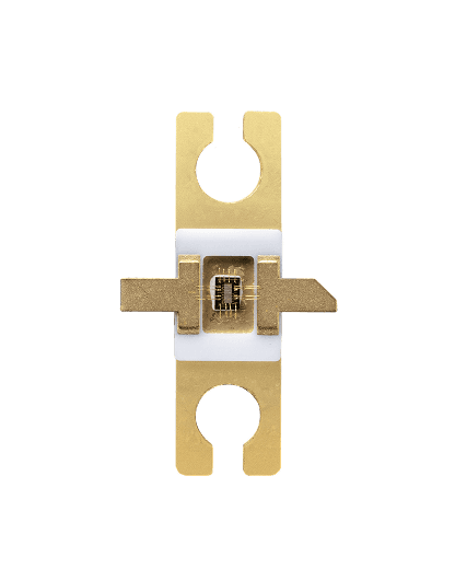
Nearly every 5G base station in the world runs on a semiconductor India barely made: gallium nitride. The material handles high power at high frequency — it is what lets radar see farther and base stations push more data — and almost all of India’s GaN components were imported, from an export-controlled supply chain. In Bengaluru, a seven-founder spinout from the Indian Institute of Science is trying to change that: AGNIT Semiconductors builds GaN wafers, RF transistors and power-amplifier modules on a MeitY-funded pilot line inside IISc itself.
AGNIT is the sharp end of a wider Indian bet on gallium nitride — a shared national fab at IISc, a defence R&D establishment making indigenous GaN HEMTs, and an announced commercial-scale GaN facility in Nava Raipur. This is what the ecosystem looks like, and how real each piece is.
Why gallium nitride matters
Gallium nitride is a wide-bandgap semiconductor: it switches faster and tolerates higher voltages and temperatures than silicon. In practice that makes it the material of choice for the RF power amplifiers in 5G base stations, for defence radar and electronic warfare systems, for satellite communications — and, on the power side, for fast chargers, EV chargers and data-centre power supplies. GaN typically handles applications below about 650 volts; silicon carbide dominates above 1,200 volts, as in EV inverters. For the wireless world, GaN is the standard.
From 15 years of IISc research to real chips
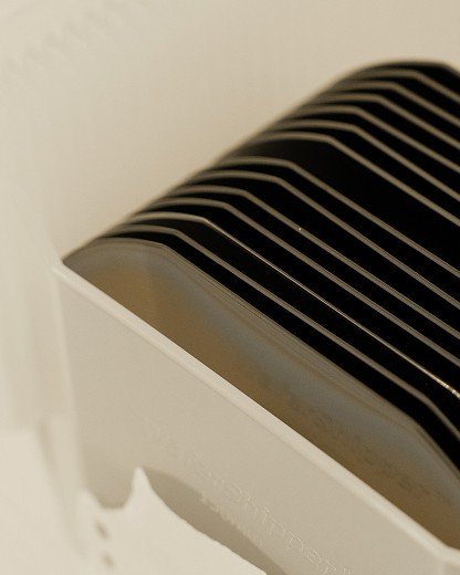
AGNIT Semiconductors was founded by seven IISc researchers, including CEO Hareesh Chandrasekar and CTO Digbijoy Neelim Nath, out of 15 to 17 years of gallium nitride research at the institute. Operational since about 2021, the company is fab-lite: it manufactures inside the IISc GaN facility. Its catalogue, per its own site, spans GaN epi wafers (gallium nitride films on silicon carbide and on silicon), discrete GaN RF transistors, power-amplifier modules from S-band to X-band, and evaluation boards. In an interview with EE Times, the company described a current RF product portfolio spanning 5W to 60W of output power, with a roadmap toward 200–300W devices — a plan, not a shipped product.
The iDEX defence contract
The milestone that moved AGNIT from lab to mission came in December 2023: the 300th contract under the Ministry of Defence’s Innovations for Defence Excellence programme, signed with M/s Agnit Semiconductors Pvt Ltd, for the design and development of advanced GaN semiconductors for next-generation wireless transmitters in defence — from radars to electronic-warfare jammers — using indigenous GaN technology. The press release (PIB PRID 1981593) put India’s defence establishment behind a home-grown GaN supply.
The commercial picture is still early. The company told The Hindu BusinessLine in March 2026, while raising a $2.6-million seed extension led by Shastra VC, that three distinct RF products were in pilots across Indian defence platforms — an attributed claim — and said it plans to move two of those to volume production, begin telecom RF chip pilots, and field-validate a GaN power device. Commercial shipments of its first products are targeted for July 2027: a stated plan, not delivered hardware. The funding is earmarked to scale toward one lakh GaN components over 24 months. This is a startup mid-climb, not a finished success.
More Read

GEECI: the shared fab behind the startups
What makes AGNIT’s fab-lite model possible is GEECI — the Gallium Nitride Ecosystem Enabling Centre and Incubator at IISc’s Centre for Nano Science and Engineering. It is a MeitY-funded, ₹300-crore small-volume semiconductor facility for GaN wafer deposition, device fabrication, characterization and packaging, run by IISc’s Foundation for Science, Innovation and Development. Equipment maker Oxford Instruments installed a full plasma-processing suite there for its GaN Power and RF pilot line. AGNIT is its first incubatee; in April 2025 GEECI launched an Entrepreneur in Residence programme to pull more GaN research toward commercialisation. Call it a pilot line, not a foundry — it is development-scale infrastructure, but it is exactly the shared layer India’s GaN startups were missing.
Polymatech’s Nava Raipur bet: announced, not yet built
The largest GaN announcement belongs to Polymatech Electronics, a real and substantial opto-semiconductor manufacturer — the company reported FY25 revenue of ₹1,912.13 crore from LED chips, sapphire wafers and related products, and unveiled a high-power UV-LED platform in December 2025. In April 2025, the Chhattisgarh chief minister laid the foundation stone for its proposed ₹1,143-crore GaN-based semiconductor chip and advanced-packaging facility at Nava Raipur — the first announced commercial-scale GaN investment of its kind in India.
Honesty requires the caveats: no verified 2026 production has been confirmed for the facility, and the first phase is centred on advanced packaging — Polymatech’s own GaN chip fabrication is still to come. The announced “first” framing is also disputed: GEECI’s MeitY pilot line and DRDO’s limited GaN device production predate it. As a hardware bet it is the biggest in the country; as a production story it is still a foundation stone.
The national picture
Beyond the startups, the state is in the game directly. DRDO’s Solid State Physics Laboratory developed indigenous processes for 4-inch silicon-carbide wafers, fabricated GaN HEMTs up to 150W and MMICs up to 40W at X-band, and operationalised limited production capability at GAETEC, Hyderabad — targeting strategic systems, space, aerospace, 5G and satellite communications (Defence Ministry, 2026). Above it all sits Semicon 2.0, approved in July 2026 with a ₹1,27,500-crore outlay, of which a gallium-nitride micro-LED display fab is one of the approved projects.
Key takeaway
Key takeaway: India’s gallium nitride story is unusually honest about where it stands. AGNIT has real chips, real wafers and a real defence contract — but its first commercial shipments are still a 2027 target. GEECI is genuine shared infrastructure, not a foundry. Polymatech’s facility is the biggest GaN announcement in the country and still a foundation stone. The material for 5G and radar is finally being made in India; the volume isn’t here yet. That gap is the story to watch.