

For half a century, chips got faster the same way: by shrinking the transistor. Smaller transistors, packed tighter, switching quicker. That road is now running out of room — transistors are approaching atomic limits, and the cost of each new shrink keeps climbing. So the industry is turning the chip on its side. Instead of spreading components across a flat die, the chips of the future will be stacked — logic on memory on I/O, like floors in a skyscraper, with data travelling vertically instead of across a crowded plain.
The stacking itself is no longer the hard part. The hard part is designing the stack. Every floor changes the heat, the timing and the stress on every other floor, and the tools chip engineers have used for decades were built for flat chips. That is the problem a Bengaluru startup called Archgen Labs has set out to solve — with an AI agent that designs the chip, run by run, the way a senior engineer would, only faster.
Archgen Labs was founded in 2026 by Hariharan Ayappane and Naveen Venkat, and it is part of Y Combinator’s Fall 2026 batch. The company’s ambition, stated plainly on its own pages, is to make chip design 1,000 times faster. Its flagship product is Newton, an AI agent for physical chip design, and in November 2026 the company launched it publicly alongside the rest of its stack.
The wall 3D chips hit
Stacking dies sounds simple until you try to design one. In a flat chip, a place-and-route tool worries about two dimensions: area, timing slack and the power grid. In a 3D stack, silicon dies are thinned to micrometres and joined by hundreds of thousands of microscopic through-silicon vias and copper micro-bumps, and every decision ripples through the whole tower. A hot logic die buried under memory changes what will close. A path that starts on one tier and ends on another has to meet timing across the bond. Heat has nowhere easy to go.
Engineers have coped by closing the stack by hand — weeks of manual iteration across separate thermal, electrical and layout tools, each pass checked, tweaked and re-run. India knows this bottleneck intimately: the country is home to roughly a fifth of the world’s chip-design engineers, yet the electronic design automation software they work with has historically belonged to a handful of overseas companies. Building sovereign EDA tools is now an explicit priority of the India Semiconductor Mission, and Archgen is building exactly that kind of tool.
Newton, the agent that reads every run
Newton is Archgen’s answer to the manual grind. It is an autonomous agent that works through the full physical-design flow — from synthesis through floorplan, placement, clock-tree synthesis, routing, timing and design-rule signoff, all the way to 3D stacking. As the company puts it, the agent “reads every run, finds why a block is failing, patches the flow and reruns. What worked carries over to the next block, on one die or across a stack.”
More Read

In practice, that means Newton reads the reports each design run produces, traces a failure to its cause — an SRAM macro sitting too far from its arbiter, congestion crowding the macros, a timing path that will not close at the target utilisation — changes the design, and queues the rerun itself. It tests candidate changes, rejects the weak ones before expensive checks, and carries verified results forward. The same loop that fixes one block gets smarter for the next one.
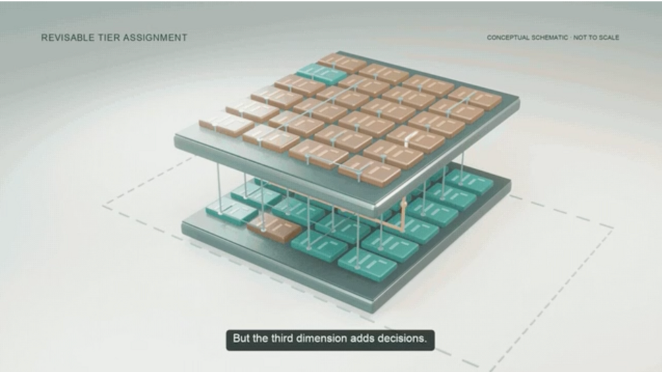
Archgen Labs’ 3D chip stack concept: logic, memory and I/O as stacked tiers, designed as one system. (Image: Archgen Labs)
Heat, predicted in milliseconds
The second piece of Archgen’s stack tackles the problem that makes 3D design so unforgiving: heat. The company’s LayerTherm tool uses physics-informed neural networks to predict a chip’s temperature map from its power distribution. In the company’s own benchmarks, a prediction that takes conventional EDA solvers 314 seconds arrives in 62 milliseconds — roughly 5,000 times faster. That speed matters because it lets engineers screen far more candidate designs for hotspots before committing to detailed thermal verification.
Underneath it all sits Archgen’s GPU-accelerated placement engine, which decides which components belong on each layer, shortens the critical connections between them, and weighs timing against temperature as it goes. The engine has already proved itself in the open: it ranked first globally in the macro-placement challenge run by Hudson River Trading and Partcl, competing against more than 120 teams from around the world.
From Bengaluru to the world’s foundries
Archgen is not building in a vacuum. The company says it has signed pilot projects with customers, and it is working with GlobalFoundries on 3D chip development, targeting its first tapeout — the moment a finished design is sent for manufacturing — in 2027. Its earliest believers include the Mercatus Center at George Mason University and Emergent Ventures, whose $15,000 grant helped the two founders incorporate and buy the cloud compute for their first experiments.
The opportunity is enormous. The global EDA market is projected to reach $24.07 billion by 2030, and every AI accelerator, every high-bandwidth-memory stack and every 3D chip that follows will need tools that can design in three dimensions. Archgen’s bet is that those tools can be built by a small team of Indian engineers — two founders, a handful of colleagues, a Bengaluru base and a Y Combinator backing — and that the agent doing the designing can learn, run after run, until the hardest part of building a chip is simply describing what you want it to do. If Newton delivers on that promise, the skyscrapers of silicon will have been designed, floor by floor, by an AI that never sleeps.
Keep reading: The Gurugram Teenager Who Cracked Apple’s AirPods Code: Inside LibrePods, the App Freeing AirPods From the iPhone · The Robot That Pulls 4,600 kg: Inside Ati Robotics, the Bengaluru Startup Automating the World’s Factories · More Industrial Automation & Technology stories
Like stories like this? Add Exceptional Technology as a preferred source on Google to see more of our reporting in your search results and Discover feed.